Company Profile
| Company name | CUSIC Inc. |
|---|---|
| Founding | November 13, 2014 |
| Capital | 2,500,000 JPY |
| Services | Technology consulting Market research and business planning Consignment study Patent consulting Design and prototyping of experimental devices Arranging and conducting of seminars, lectures, and short course |
| Directors | Representative director Hiroyuki Nagasawa Director Ryo Mimura Outside Director Shinichi Mitani |
| contact | Email: contact@cusic.co.jp |
Competency of CUSIC
- Using international network, CUSIC adapts cutting-edge technologies to client’s business.
- CUSIC responds immediately for emerging trouble of client’s production system as well as for long term business development.
- CUSIC synthesizes technology, intellectual property, and alliance strategy for preparing and/ or improving the client’s business plan.
Profile of senior consultant
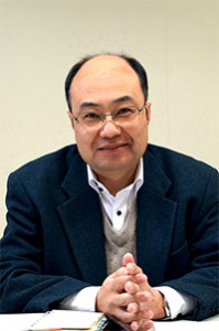
Dr. Hiroyuki Nagasawa
| 1987 | He entered Toshiba Corporation as an engineer of VLSI processing technology. He transferred the developed processing technology from laboratory to mass production plants. |
|---|---|
| 1989 | He entered material development laboratory, Hoya Corporation. He developed a thin SiC film deposition technology for implementing the x-ray lithography. |
| 1991 | He developed an atomic layer epitaxy technology for forming mono-crystalline 3C-SiC film on six inches Si substrates. This was largest record of mono-crystalline SiC diameter at that time. |
| 1997 | He got a degree of Doctor of Engineering. The thesis title for doctorate is ‘Mono-crystal 3C-SiC formation through atomic layer epitaxy’ |
| 1998 | He developed a technology for growing mono-crystalline bulk 3C-SiC. He invented unique technologies for enhancing the epitaxial growth rate and reducing the defect density. |
| 2002-2006 | He established Hoya Advanced Semiconductor Technologies corporation (HAST) as one of the founders. He promoted development of 3C-SiC bulk growth technology. HAST started production of 3C-SiC wafers. He also started 3C-SiC MOSFET and GaN/SiC HEMT developments collaborating with partner laboratories. |
| 2006 | He developed an advanced homo-epitaxial technology for reducing extended defects in 3C-SiC. This results in implementation of Normally-off 600V power switching MOSFET with highest channel mobility of 370cm²/V/sec. |
| 2013 | He joind Tohoku University, Research institute of electric communication, as a visiting professor. He is managing research project of SiC and Graphene. |